-
https://en.wikipedia.org/wiki/Semiconductor_device_fabrication
-
https://hacker-fab.gitbook.io/hacker-fab-space/fab-toolkit/patterning
-
Making Semiconductors more Conductive by introducing Partially Filled States
Currently:
learn how pn junction works, diode, transistor, fet
Manufactoring
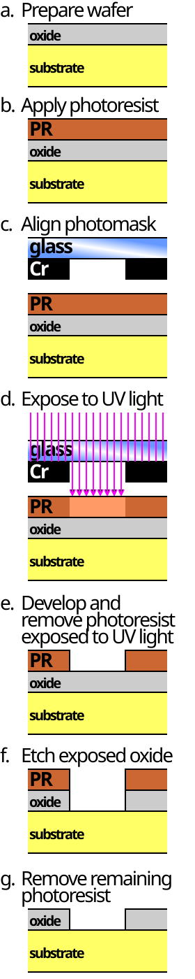
Photolithography
-
Used to draw a pattern onto a silicon wafer.
-
Followed by etching where we make the drawings physical.
-
Starts off by coating the silicon substrate in a layer of photoresist.
- Photoresist is a light sensitive chemical that either hardens (negative) or becomes soluble (positive) when exposed to light.
- The photoresist is applied evenly on the wafer using a spin-coater.
- A spin coater is like a vinyl music player.
- We put a few drops of the spin coater in the center of the wafer and spin it.
- All the excess photoresist flies off the wafer, forming a thin layer of the resist.
-
We then expose the photoresist to a pattern of intense light.
- The exposure to light causes some chemical reactions on the photoresist which, depending on whether it’s a positive or negative photoresist, weaken or harden the layer of photoresist exposed to the light.
- The light is shined onto the substrate in a pattern made by using a photomask (patterned covering).
-
After exposure, we remove some of the photoresist using a developer solution.
- Surface exposed to light when using positive photoresist becomes soluble.
- While the unexposed surface remains soluble if using negative photoresist.
- The developer solution is also delivered on a spinner like photoresist.
- The section of substrate exposed cuz of removing the photoresist is the part that gets etched away.
-
After the photoresist is no longer useful it is removed from the substrate using a resist stripper that chemically alters the resist such that it no longer sticks to the substrate surface or using plasma ashing (using oxygen to oxidize the resist).
Etching
-
Etching converts the drawn patterns to traces (think pcb) on the substrate.
-
Etching Illustrated (why are we etching oxide over the substrate?)
-
Not yet sure why we do etching. I’m guessing it provides pathways for current to flow through. Pathways we can control.
Wet Etching
- After removing sections of photoresist, we immerse the material in an etchant solution to essentially eat away the layer of oxide exposed.
- Wet etching seeps (smth like that) underneath the layer of photoresist and etches away sections it’s not supposed to.
- This tendency to get under the resist is called bias.
- Isotropic etching (when effectiveness of etching is same regardless of direction) leads to high bias. We want etching toward/under resist to be low (orientation dependent etching).
Plasma Etching (dry)
- We make plasma by using RF to ionize gas in a vacuum chamber.
- The ions are then accelerated to the surface of the substrate. Now:
- Physical Etching (sputtering): we literally blast the surface with ions which physically remove the atoms of the oxide by transferring momentum. I’m guessing this is the one done in low pressure.
- Chemical Etching: stuff in the plasma reacts with the surface material.
Depositon
rewatch: https://www.youtube.com/watch?v=-DkpxxMGY-I
Annealing
- Healing?